
Crystals used in applications as diverse as lasers, LEDs and semiconductors used in sensors found in astronomical instruments could one day be ‘drawn’ instead of ‘grown’, leading to better performance and lower costs.
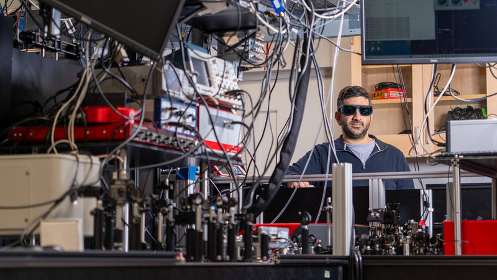
A team led by Elad Harel of Michigan State University used a laser to heat a gold nanoparticle, which then triggers crystal formation within a lead halide perovskite solution. By moving the gold nanoparticles, again using a laser, it is therefore theoretically possible to precisely ‘draw’ the crystals exactly where they need to be in an electronic device.
“The device may require a very small amount of crystalline material placed in very specific locations,” Harel told Space.com.
Harel’s new technique, using a phenomenon known as ‘plasmonic heating’, can restore some of the control over crystal formation. In laboratory experiments, Harel’s team fired a 660-nanometer laser wavelength on a gold nanoparticle in a reaction chamber filled with a lead halide perovskite precursor solution over a borosilicate glass substrate, onto which the crystal would be ‘patterned’.
A gold nanoparticle is tiny, less than one-thousandth the width of a human hair. Therefore, the entire process must be extremely precise and can be observed in real time using a high-speed microscope with sub-millisecond frame rates.
“The reason we use gold nanoparticles is that they act as little heaters,” Harel said. “When a laser irradiates a particle at the right frequency, it causes electrons in gold to oscillate, which creates heat.”
This is plasmonic heating, and it triggers the crystallization of the precursor solution in the exact places Harel’s team wants.
Lead halide perovskite crystals show high performance in solar cells and LEDs, but they are not the only type of crystal used in electronics. For example, semiconductors in the Mid-Infrared Instrument (MIRI) at The James Webb Space Telescope they contain silicon crystals doped with arsenic. Harel hopes that this plasmonic heating technique can be applied to other such crystals, but it works specifically for lead halide perovskites because they have some rather unusual properties.
“What’s special about these perovskites is that as the temperature increases, the solubility decreases, which induces crystallization,” he said. “Most materials do not exhibit this property of retrograde solubility; typically as temperature increases, solubility increases.”
However, there may be a way around this that lies in the jittering of the excited electrons. In addition to producing heat, electrons could in principle also participate directly in the chemistry of crystal formation, according to Harel, promoting crystal formation.
“We need to do more work to generalize this concept to other materials, but we believe it will work,” he said.
The advantages of cheaper, faster and more precise crystal formation are clear. Crystals are used everywhere from touch screens, smoke alarms, solar panels, medical imaging devices and most optoelectronics and photodetectors in general.
“This is a very simple method that uses cheap lasers,” Harel said. “It also saves enormously on manufacturing costs because the crystal can be placed exactly where and when needed.”
Given the importance of crystals for astronomical sensing, the technique of drawing them could lead to the launch of cheaper instruments on future space missions.
The next step is to use multiple lasers at different wavelengths to try to ‘etch’ more intricate crystal patterns and then start testing them in real devices to see if they really offer a better standard of performance for less cost. “This is something we’re working on right now,” Harel said.
This new technique of ‘drawing’ crystals was published in the journal ACS Nano.
Source link
Technology , , #Scientists #discover #grow #materials #demand #crystals #light, #Scientists #discover #grow #materials #demand #crystals #light, 1761220326, scientists-discover-a-new-way-to-grow-materials-on-demand-using-crystals-and-light